File:MicroChipAtomicTrap00.jpg
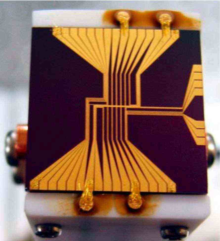
Historical photo of the first microchip atomic trap.
Previously, this file appeared at http://commons.wikimedia.org/wiki/File:MicroChipAtomicTrap00.jpg
Copyleft 2003 by Ken-Ichi Nakagawa.
Descriprion
The first microchip atomic trap, designed at the ILS, Japan. The structure of wires is painted with gold at the insulator substrate. The main wire has Z-shape; the magnetic field allows the trapping of neutral atoms due to their magnetic momentum. The chip has sizes 2 x 2 cm. It was placed to the uniform magnetic field (source of this field is not shown in the picture); the traping is realized for so-called "atoms seeking for low magnetic field". The only atoms with positive spin-field energy were trapped. The miminim of the field is realized at the side of the chip, close to the central part of the z-electrode with electric current.
The movement of atoms along the wire is limited by the angles of the "Z". Additional electrodes were designed to play with the effective potential along this wire. The interaction with laser beams and reduction of the trapping potential allow the additional cooling of atoms (coling with evaporation), reaching the BEC. In the shown design, the only one additional electrode is supplied with contacts. It was planned to use other electrodes to modify the potential in experiments with single-dimentional quantum mechanics. Actually, more advanced microchip atomic traps were manufactured instead.
In principle, such devices could trap also neutrons, giving raise to the new branch of research, namely, nuclear physics of low energies. Up to year 2011, the main problem with trapping of neutrons is the primary cooling, say from few Kelvin (which is realizable in cold Beryllium and/or heavy hydrogen targets) to microKelvin (that allows to handle neutrons using their spin).
References
http://www.ils.uec.ac.jp/Eatomoptics.html Atom Optics, Coherence and Ultra Cold Atoms" at the Institute for Laser Science
M.Horikoshi; K.Nakagawa (2006). "Atom chip based fast production of Bose-Einstein condensat". Applied Physics B 83: 363-366.
File history
Click on a date/time to view the file as it appeared at that time.
| Date/Time | Thumbnail | Dimensions | User | Comment | |
|---|---|---|---|---|---|
| current | 17:50, 20 June 2013 | | 890 × 976 (44 KB) | Maintenance script (talk | contribs) | Importing image file |
- You cannot overwrite this file.
File usage
The following 3 pages link to this file: